01005 Packages · 0.2mm Pitch BGA/QFP PCB Assembly: Technical Breakthroughs and Quality Assurance
When Miniaturization Meets High Reliability: The New Frontier of Electronics Manufacturing
Monitoring ECG activity in a smartwatch the size of a fingertip, enabling wireless communication in an implantable device smaller than a grain of rice—modern electronic products are advancing into the microscopic world at an unprecedented pace. This trend has introduced two component types that make traditional manufacturers hesitate: 01005 packages (0.4mm×0.2mm) miniature passive components and 0.2mm pitch BGA/QFP high-density chips. When a 01005 resistor measures less than one-third the size of a sesame seed, and BGA solder ball spacing equals just three human hairs placed side by side, PCB assembly transcends simple manufacturing—it becomes a systematic engineering challenge that pushes physical boundaries.
Technical Abyss: The Invisible Barriers of Micro-Component Assembly
01005 Packages: Challenges Too Small to See
01005 components (0.4mm×0.2mm) face triple physical limitations:
- Visual limits: Component dimensions approach the human eye resolution limit (0.1mm), making precise identification difficult for conventional vision systems
- Mechanical limits: Component weight under 0.001g makes them susceptible to electrostatic and airflow interference, with placement tolerance <25μm
- Thermal limits: Minor thermal capacity differences across microscopic pads easily cause "tombstoning" during reflow, with traditional process yields <70%
0.2mm Pitch BGA: The Balancing Act of Precision and Reliability
The assembly challenges of 0.2mm pitch BGA packages are even more complex:
- Stencil challenges: Requires ±3μm aperture accuracy with area ratios >0.66 to ensure proper solder paste release
- Coplanarity difficulties: Solder ball height tolerances must be controlled within 10μm to prevent open circuit risks
- Thermal management dilemma: Dense solder joints create uneven heat distribution, making traditional reflow profiles inadequate for all joints
- Inspection difficulties: X-ray detection requires <1μm resolution to identify micro-bridging between adjacent solder balls
Breaking Barriers: FR4PCB.TECH's Systematic Solutions
Ultra-Precision Manufacturing Systems
Intelligent Placement Platform: Pick-and-place machines equipped with sub-micron linear encoders and 12MP high-resolution vision systems maintain ±10μm placement accuracy even in mixed 0402/0201 environments. For 01005 components, innovative adaptive vacuum pickup technology monitors suction force in real-time (0.1g precision), eliminating component damage and misplacement risks.
Nano-level Printing Process: 75μm thick laser-cut nano stencils with trapezoidal aperture walls, combined with closed-loop pressure control systems, achieve solder paste volume consistency with CpK>1.67. 3D SPI inspection systems complete 100% pad coverage analysis within 3 seconds after printing, automatically isolating abnormal boards.
Zoned Thermal Control: 12-zone nitrogen reflow ovens (oxygen content <50ppm) equipped with AI thermal distribution optimization systems implement independent thermal profiles for 0.2mm BGA areas. Micro thermocouples measure actual BGA bottom temperature distribution, ensuring differentials <3℃ and void rates controlled below 8%.
End-to-End Quality Assurance System
FR4PCB.TECH has established a rare four-tier inspection mechanism in the industry:
- 3D SPI: 100% inspection of solder paste volume, height, and positional accuracy
- High-Resolution AOI: 5μm pixel resolution identifies component misalignment, tombstoning, and missing parts
- 3D X-ray Inspection: 1μm resolution phase-contrast imaging technology precisely identifies BGA internal voids and micro-bridging
- Selective Cross-section Verification: Non-destructive cross-sectioning of critical areas validates internal structural integrity
Specifically for high-reliability applications in medical and aerospace fields, we implement single-board lifecycle tracking, recording 218 process parameters and inspection results for each PCB, ensuring complete traceability.
Real-World Validation: European Cardiac Monitoring Device Success Story
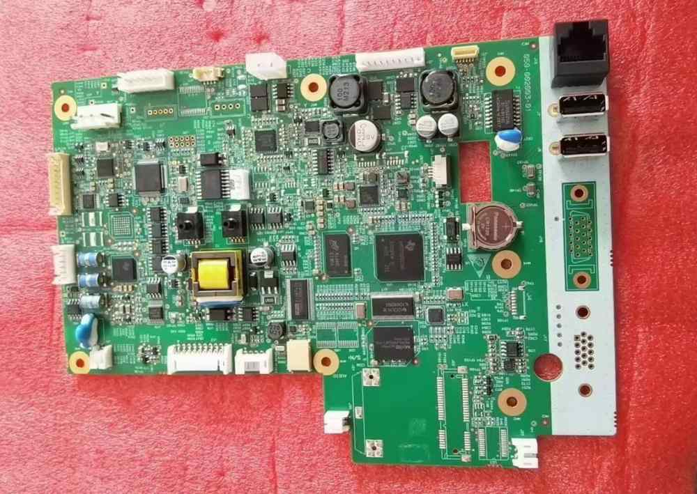
A leading European medical device manufacturer was developing an implantable ECG monitor facing the daunting challenge of integrating a 32-channel acquisition system within an 8×8×2mm space. The design contained 478 01005 components and two 136-ball 0.2mm pitch BGA processors, achieving component density of 185 units/cm².
Challenge: The client needed to complete the journey from prototype to FDA certification within 24 months, with first production run yields >95% to meet strict medical certification timelines.
FR4PCB.TECH's Solution:
- Customized independent thermal zones for different component density areas, resolving conflicting thermal requirements between BGAs and micro-components
- Developed specialized flexible board support fixtures eliminating 0.05mm-level deformation during reflow
- Implemented intelligent component moisture management systems, applying J-STD-033D standards to 01005 components
Results: Initial 500-unit production achieved 98.7% yield rate, with BGA solder joint void rates controlled below 8%, helping the client obtain FDA 510(k) certification 45 days ahead of schedule. More critically, rigorous process capability analysis (Cp/Cpk>1.67) established a reliable foundation for volume production at 100,000 units monthly.
Engineer's Guide: Practical Advice for High-Density PCB Design
To help design engineers improve manufacturability of miniaturized products, we summarize these key DFM principles:
-
Pad Design Optimization:
- 01005 components: Recommend NSMD pad design, dimensions 0.23×0.13mm
- 0.2mm BGA: Use solder mask defined (SMD) pads, diameter 0.11mm, solder mask opening 0.15mm
-
Stencil Design Essentials:
- 01005 areas: Stencil thickness 60μm, area ratio >0.75
- 0.2mm BGA areas: Use step stencils with center areas reduced to 50μm thickness
-
Layout Strategy:
- Avoid placing tall components within 3mm of 0.2mm BGAs to ensure X-ray inspection angles
- Group 01005 components together to reduce time wasted on frequent nozzle changes
-
Material Selection:
- Prioritize low-roughness substrates (≤0.5μm) with ultra-flat copper foil
- Select high-frequency materials with Tg>170℃ to reduce Z-axis expansion during reflow
The Future Is Here: Cutting-Edge Technologies in Miniaturization Manufacturing
Industry frontiers are already exploring 008004 components (0.25×0.125mm) and 0.15mm pitch BGA manufacturing processes. These technologies require breakthrough solutions:
- Wafer-Level Direct Integration: Bypass traditional packaging to directly integrate bare dies on PCBs
- Microfluidic Solder Paste Deposition: Replace conventional stencil printing with nanoliter-level precise control
- Selective Laser Soldering: Apply localized precise heating to critical solder joints
- AI-Driven Real-Time Process Adjustment: Dynamically optimize process parameters based on inline inspection data
Conclusion: Freeing Innovation from Manufacturing Limitations
In electronics manufacturing, process capability often defines the boundaries of product innovation. When a designer creates a revolutionary product with 01005 components and 0.2mm BGAs in CAD software, they need more than just a manufacturer—they need an innovation partner capable of turning impossibility into reality.
FR4PCB.TECH is committed to becoming the solid backbone of electronics innovation by continuously investing in cutting-edge equipment, cultivating specialized talent, and optimizing processes to constantly expand manufacturing boundaries. We believe that only when design imagination seamlessly connects with manufacturing possibility can we truly unlock the innovative potential of electronic products, transforming world-changing ideas from drawings into reality.
Miniaturization isn't the destination—reliability is. While pursuing extreme miniaturization, we always prioritize product reliability because the tiniest devices often carry the most critical missions.


