FR4PCB.TECH offers small-batch PCB assembly services, with core strengths including process adaptability, quality compliance, efficient delivery (within 48 hours), and cost optimization (as low as $0.02 per solder joint). Leveraging full-process quality control and precise process adaptability across multiple fields, we provide free Design for Manufacturability (DFM) analysis and customized solutions. For inquiries, please contact us via email at info@fr4pcb.tech.
Small-Batch PCB Assembly: The Foundation of Electronic Innovation and the Blueprint for High-Quality Delivery
I. Introduction: Why Small-Batch PCB Assembly Has Become a Must-Have for Modern Electronics Enterprises
Against the backdrop of the ever-shortening innovation cycles and increasingly diversified market demands in the global electronics industry, small-batch PCB assembly has evolved from a "transitional phase before mass production" into a strategic pillar supporting enterprise development. It plays a crucial role in scenarios such as new product research and development verification, the first trial production of start-up companies, the manufacturing of industrial customized equipment, and the supply of small-batch personalized products. Its core values—flexible iteration to adapt to design adjustments, cost control to reduce trial production risks, and rapid delivery to seize market opportunities—precisely meet the urgent needs of current electronics enterprises.
However, the small-batch PCB assembly market is fragmented, and many enterprises encounter significant bottlenecks. Large manufacturers often overlook small-batch orders, resulting in extended lead times of 7-14 days. Small workshops, while accepting small orders, frequently suffer from quality issues such as cold solder joints, incorrect component placement, and non-compliance with international standards due to a lack of standardized processes and advanced equipment. These problems not only delay product launch schedules but also increase overall research and development and production costs. Therefore, high-quality small-batch PCB assembly has become a key competitive edge for enterprises to stand out in the fierce market competition, enabling them to achieve a balance between precision, compliance, efficiency, and cost-effectiveness.
II. Core Keywords of High-Quality Small-Batch PCB Assembly: Decoding the Success Factors
1. Process Adaptability: Meeting Diverse Customization Needs
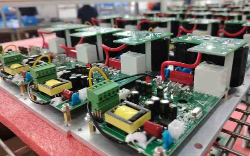
High-quality small-batch PCB assembly must break free from the limitations of single-process production and achieve full coverage of complex process requirements. It needs to be compatible with a hybrid assembly of surface mount technology (SMT) and through-hole technology (THT), efficiently handle ultra-miniature 01005 packages, 0.4mm pitch ball grid arrays (BGAs), and other fine-pitch components, and support special processes such as conformal coating (for moisture, corrosion, and dust protection) and vibration-resistant spot gluing. This adaptability ensures that various personalized and complex product design requirements are accurately transformed into physical samples or finished products.
2. Quality Compliance: Building a Solid Foundation for Market Access
In the global market, compliance is the basic threshold for products to enter international markets. High-quality small-batch PCB assembly must strictly adhere to international standards such as the Restriction of Hazardous Substances Directive (RoHS 3.0), the Printed Circuit Board Manufacturing Standard (IPC-A-600H), and the Solder Material Standard (IPC-J-STD-006). It should implement lead-free production throughout the entire process, strictly control the content of harmful substances such as lead, cadmium, and phthalates, and provide third-party testing reports to ensure that products meet the environmental and quality requirements of different regions, thereby removing market access barriers for enterprises.
3. Efficient Delivery Capability: Accelerating Product Launch Rhythms
The core demand for small-batch PCB assembly lies in "speed," which directly affects product research and development iteration and market entry efficiency. High-quality services rely on flexible production lines and efficient supply chain collaboration to compress the entire production cycle. From Gerber file review, material preparation, assembly, to testing, they can achieve rapid delivery within 48-72 hours, far exceeding the average industry lead time, helping enterprises quickly verify product feasibility and seize market windows.
4. Cost Optimization: Reducing the Burden of Small-Batch Production
Small-batch orders often face the problem of relatively high unit costs, and high-quality services can solve this pain point through scientific management. By adopting a transparent pricing model (e.g., lead-free surface mount services as low as $0.02 per solder joint), eliminating high mold opening fees and minimum order quantity restrictions, and optimizing the procurement chain and production efficiency, they can reduce the trial production and small-batch production costs for enterprises while ensuring quality, especially benefiting start-up companies and research and development teams with limited budgets.
III. Technical System of High-Quality Small-Batch PCB Assembly: Full Control from Incoming Materials to Finished Products
1. Incoming Material Quality Control: Guarding the Source of Quality
The quality of small-batch PCB assembly starts with strict incoming material management. Professional service providers will establish a comprehensive incoming quality control (IQC) system:
- Component Traceability: Strictly review supplier qualifications, require the provision of RoHS compliance reports and quality certificates, and implement barcode management for each batch of components to achieve full-process traceability from procurement to assembly, eliminating the use of counterfeit and shoddy components. For commonly used components such as 0402 package resistors and capacitors, additional X-ray fluorescence (XRF) spot checks are conducted to ensure that the content of harmful substances is below the limits specified in RoHS 3.0 (lead ≤ 1000 ppm, cadmium ≤ 100 ppm).
- PCB Substrate Selection: Prioritize the use of FR4 glass fiber epoxy resin substrates with a glass transition temperature (Tg) ≥ 130°C, which have excellent high-temperature resistance and mechanical strength, suitable for the high-temperature environment of lead-free soldering, preventing issues such as PCB delamination and deformation. For industrial-grade products, high heat-resistant substrates with Tg ≥ 170°C can be upgraded, and they should show no obvious damage after thermal shock testing (-40°C to 125°C, 100 cycles).
- Solder and Auxiliary Material Inspection: Use SAC305 lead-free solder that complies with IPC standards (with stable soldering performance and environmental friendliness), which has a melting point of 217°C and a solder joint tensile strength ≥ 45 MPa, and is paired with ROL0-grade no-clean flux with a solid content of 20%-30% to reduce solder joint oxidation and residual contamination, ensuring soldering reliability.
2. Core Process Implementation: Precision in Details
The core of small-batch PCB assembly lies in the precise execution of each process. Professional service providers will strictly control every link:
- Pre-production Design for Manufacturability (DFM) Optimization: Within 2 hours of receiving the customer's Gerber files and bill of materials (BOM), conduct a comprehensive design for manufacturability review, optimize parameters such as line width (minimum support of 3 mil), pad size (adjusted according to IPC-7351 standards), and hole diameter (minimum of 0.2 mm), and promptly communicate with the customer to adjust unreasonable designs to avoid production problems caused by mismatches between design and process.
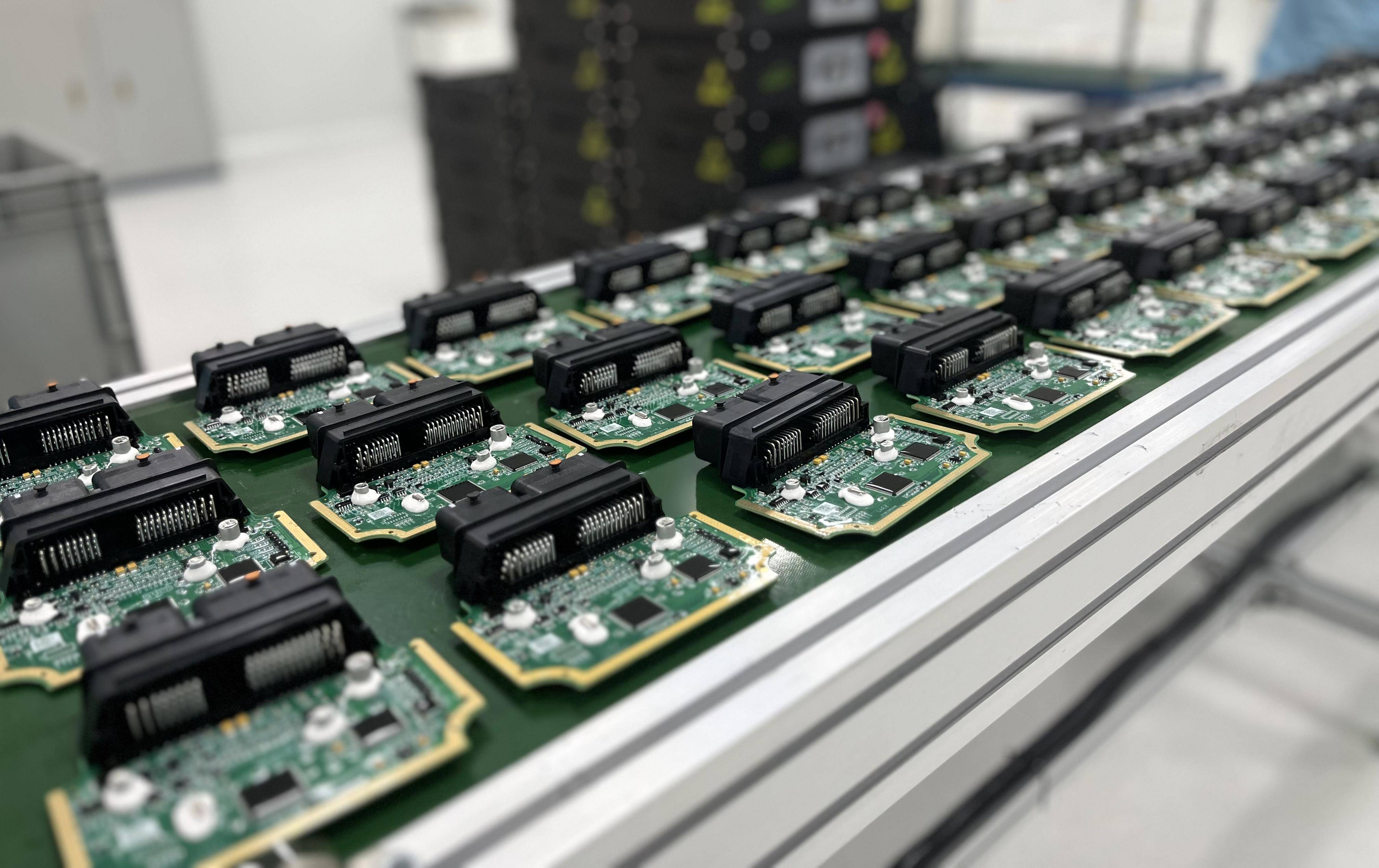
- High-Precision Component Placement: Equipped with high-speed and high-precision placers such as the Panasonic NPM-D3, with a placement speed of 46,000 components per hour (CPH), it can accurately handle ultra-miniature 01005 components (0.4 mm × 0.2 mm) and 0.4 mm pitch BGA components, with a placement accuracy of ±30 μm/3σ. For irregular components such as connectors and sensors, custom nozzles are used and visual positioning technology is adopted to ensure placement accuracy, with a placement yield exceeding 99.7%.
- Diversified Soldering Processes: Combine lead-free reflow soldering and selective wave soldering to meet hybrid assembly requirements. An 8-zone independently controlled temperature reflow oven can customize a stepped temperature profile according to component types (preheating at 150-180°C, peak temperature at 240-250°C, cooling rate of 5-8°C/s), controlling the void rate of solder joints within 5%. A selective wave soldering machine uses custom shielding fixtures and precisely controls the soldering temperature at 255 ± 5°C, with a pin wetting rate ≥ 95%, avoiding secondary heating of surface mount components.
- Post-Processing Protection: Provide post-processing services such as conformal coating and spot gluing according to the product's application scenario. Conformal coating uses acrylate, polyurethane, or silicone materials with a coating thickness of 20-50 μm, enabling the product to pass the IP65 protection level test and show no corrosion after a salt spray test (5% NaCl solution, 48 hours). The spot gluing process uses thermal conductive adhesive with a thermal conductivity of 0.8-1.2 W/(m·K), and after curing, the shear strength is ≥ 1.5 N/mm², improving the mechanical stability of core components and being suitable for vibration environments such as automotive and industrial applications.
3. Full-Process Quality Inspection: Ensuring Zero-Defect Delivery
High-quality small-batch PCB assembly requires the establishment of a closed-loop quality inspection system to eliminate defects at each stage:
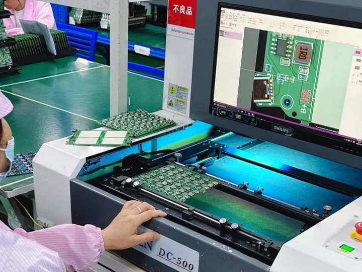
- Online Inspection: After solder paste printing, use a 3D solder paste inspection (SPI) device with an accuracy of ±1 μm to detect printing quality, covering parameters such as solder paste thickness, area, and offset. After component placement, use an 8-view imaging 3D automatic optical inspection (AOI) device to identify missing components, wrong components, and offsets, with a false rejection rate ≤ 0.1%. After soldering, use an X-ray inspection device to penetrate the solder joints at the bottom of BGAs and quad flat packages (QFPs) to Identify internal voices, cold solder joints, and other defects.
- Reliability Testing: Conduct sampling reliability testing on key products, including thermal shock testing (-40°C to 125°C, 100 cycles), temperature cycle testing (-20°C to 85°C, 500 cycles), and vibration testing (10-2000 Hz, acceleration of 10G). After testing, there should be no cracks in the solder joints and no dislodgement of components, and the product functions normally.
- Functional Verification: Customize functional circuit test (FCT) fixtures according to the customer's test specifications, covering multi-dimensional tests such as voltage (accuracy ±0.01 V), current (accuracy ±0.001 A), signal transmission, and communication protocols (e.g., I2C, SPI), with a test coverage rate ≥ 98%, ensuring that each product meets functional requirements before delivery.
IV. Application Scenarios and Value Realization: Empowering Innovation in Multiple Fields
1. Consumer Electronics R&D: Accelerating Product Iteration
In the research and development stage of consumer electronics products such as smart wearables and IoT devices, small-batch PCB assembly is crucial for prototype verification. A smartwatch manufacturer once needed 30 sets of screen driver module assemblies for functional testing. The module size was only 20 mm × 15 mm, containing a 0.4 mm pitch BGA-packaged driver chip, requiring lead-free compliance and delivery within 4 days. Relying on high-quality small-batch assembly services, PCB manufacturing and surface mount were completed within 48 hours, with zero defects detected by automatic optical inspection, and compliance reports were delivered simultaneously. This helped the manufacturer quickly locate design defects (optimizing two areas with insufficient line width), reducing the research and development cycle from the originally planned 45 days to 31 days, a 30% reduction.
2. Industrial Control Customization: Meeting Demanding Environmental Requirements
Programmable logic controller (PLC) modules, industrial sensors, and other industrial control equipment often operate in harsh environments with high temperatures, vibrations, and corrosion, placing extremely high reliability requirements on PCB assembly. An industrial sensor enterprise customized 50 sets of PLC input/output modules, involving a hybrid assembly of surface mount and through-hole technology and conformal coating requirements. The modules needed to withstand a working temperature range of -40°C to 85°C. Professional service providers optimized the design for manufacturability (adjusting the layout of 3 pads), used selective wave soldering, and automated conformal coating, completing the order delivery within 72 hours. The products passed high-temperature and low-temperature tests and 10-2000 Hz vibration tests, with a change in the connection resistance of solder joints ≤ 5%, fully meeting the reliability requirements of industrial environments.
3. Product Launch for Start-up Companies: Lowering Market Entry Barriers
Start-up companies often face challenges such as limited budgets and tight launch schedules. A smart home start-up company planned to launch its first batch of 100 smart gateway products, which contained multiple types of components such as Wi-Fi chips and Bluetooth modules, with a budget of within 50,000andarequirementfordeliverywithin10days.High−qualitysmall−batchassemblyservicessolvedthisproblemwithalead−freesurfacemountquoteof0.02 per solder joint and a 48-hour rapid delivery capability. The final trial production cost was controlled at $42,000, and complete compliance reports were provided, helping the start-up company quickly pass the review of e-commerce platforms and successfully enter the market, with first-month sales exceeding 500 units.
V. Guide to Selecting Small-Batch PCB Assembly Service Providers: Tips for Avoiding Pitfalls
- Verify Compliance Qualifications: Confirm whether the service provider can provide compliance reports for international standards such as RoHS 3.0 and IPC, and whether it has certifications from third-party testing institutions (e.g., SGS, Intertek) to ensure the product's market access capability.
- Inspect Process Equipment: Understand the service provider's equipment configuration, whether it has high-precision placers, 3D automatic optical inspection equipment, and X-ray inspection equipment, and whether it can handle fine-pitch components such as 01005 packages and 0.3 mm pitch QFPs, as well as special processes, which directly determine its production capacity.
- Confirm Delivery Capability: Inquire about the actual delivery cycle for small-batch orders and emergency order response plans, and verify them through customer cases to avoid delays caused by insufficient production capacity of the service provider. Request screenshots of the production scheduling system to confirm the response speed of the flexible production line.
- Clarify Pricing System: Understand the specific pricing model, whether there are transparent quotation standards, and whether there are hidden costs such as mold opening fees and minimum order quantity fees. You can request a detailed quotation to clarify the costs of materials, processes, testing, and other aspects to ensure cost control.
- Check Customer Cases: Request service cases and customer evaluations in relevant industries, understand the service provider's experience in handling similar projects, focus on cases similar to your own products, view their process implementation effects and delivery data, and judge their comprehensive service capabilities.
VI. Conclusion and Call to Action: Collaborating for Efficient Innovation
In the era of rapid iteration of electronic products, high-quality small-batch PCB assembly is not just a production link but a strategic partner for enterprises to accelerate innovation and seize market opportunities. Through process adaptability, quality compliance, efficient delivery capability, and cost optimization, it solves the pain points of enterprises in research and development verification, small-batch production, and customized manufacturing.
FR4PCB.TECH, as a professional small-batch PCB assembly service provider relying on a top-tier surface mount factory in China, has mature technical capabilities and service experience. We support hybrid assembly of surface mount and through-hole technology, handling of fine-pitch components, and special processes such as conformal coating, strictly adhere to international standards to ensure product compliance, and provide lead-free surface mount services at $0.02 per solder joint and 48-hour rapid delivery. We have helped thousands of enterprises in the fields of consumer electronics, industrial control, and start-ups achieve efficient product launches.
If you have needs for research and development prototype assembly, small-batch trial production, or customized PCB assembly, welcome to contact us via email at info@fr4pcb.tech. Provide your Gerber files and bill of materials, and you can get a free design for manufacturability analysis and a customized assembly plan, letting professional services empower your innovation journey!


