Common Quality Defects and Solutions in PCB Assembly
PCB assembly is a core link in electronic manufacturing. Affected by multiple factors such as design, materials and process parameters, various quality defects are prone to occur. The following sorts out high-frequency quality problems, causes and targeted solutions in PCB assembly to help improve assembly yield and product reliability.
I. Soldering Defects
1. Cold Solder Joint (Pseudo Soldering)
- Phenomenon: The solder joint appears formed on the surface, but it is not effectively bonded to the pad or pin in reality, posing risks of poor conduction or later failure.
- Causes
- Oxidation or contamination of pads/pins without cleaning treatment;
- Insufficient activity of solder paste, or excessive storage time after printing;
- Unreasonable reflow soldering temperature profile, with insufficient peak temperature or holding time;
- Placement accuracy deviation, leading to misalignment between component pins and pads.
- Solutions
- Incoming material control: Ensure that component pins and PCB pads are free of oxidation; oxidized parts should be cleaned or tinned;
- Process optimization: Select high-activity solder paste and complete placement and reflow soldering within 2 hours after printing;
- Temperature calibration: Adjust the reflow soldering profile according to solder paste specifications to ensure compliance with peak temperature and holding time requirements;
- Equipment debugging: Calibrate placement machine accuracy and control component placement offset ≤ ±0.1mm.
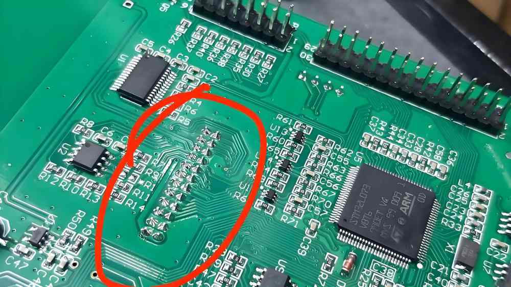
2. Solder Bridging
- Phenomenon: Adjacent pads or pins are connected by solder, causing short circuits, which is common in high-density pin devices (such as QFP, BGA).
- Causes
- Excessive solder paste printing or oversized stencil aperture;
- Placement offset, resulting in overlap between component pins and adjacent pads;
- Too fast heating rate in reflow soldering, causing solder paste to melt and spread before full wetting.
- Solutions
- Stencil optimization: Reduce stencil aperture size in high-density pin areas and adopt laser-cut stencils to improve precision;
- Printing parameter adjustment: Reduce squeegee pressure and printing speed to avoid excessive extrusion of solder paste;
- Placement calibration: Improve the recognition accuracy of placement machines for pin devices and control placement offset;
- Reflow soldering adjustment: Adopt a slow heating profile, extend preheating time, and ensure full activation of solder paste.
3. Solder Balls
- Phenomenon: Small solder particles scattered around solder joints, which may cause insulation failure or short circuits, and is a common defect in SMT assembly.
- Causes
- High metal powder content in solder paste, or excessive printing pressure squeezing solder paste outside pads;
- Unreasonable PCB pad design with too small pad spacing;
- Insufficient preheating in reflow soldering, causing flux in solder paste to splash and carry solder particles when heated without full volatilization.
- Solutions
- Select solder paste with moderate metal content (recommended 88%-90%) and optimize printing pressure;
- Design optimization: Increase pad spacing and avoid overlap between pad edges and solder mask;
- Reflow soldering optimization: Extend preheating time (generally 60-90 seconds), control heating rate ≤ 2℃/s, and ensure full volatilization of flux.
II. Component Placement Defects
1. Component Misalignment/Skewing
- Phenomenon: The center of the component is misaligned with the center of the pad, or the component body is tilted at a certain angle relative to the pad, affecting electrical performance and appearance.
- Causes
- Wear or mismatch of placement machine nozzles, leading to unstable component picking;
- Incorrect setting of placement coordinate parameters;
- Uneven solder paste printing, causing component offset due to uneven surface tension during reflow soldering.
- Solutions
- Regularly inspect placement machine nozzles, replace worn parts in a timely manner, and select appropriate nozzles matching component specifications;
- Calibrate placement coordinates and accurately locate pads through vision systems;
- Optimize solder paste printing process to ensure uniform distribution of solder paste on pads.
2. Component Reverse Polarity/Wrong Part
- Phenomenon: Reverse polarity placement of components (such as diodes, capacitors, ICs) or use of wrong component models, directly leading to product function failure.
- Causes
- Material sorting errors, mixing components of different models/polarities;
- Incorrect placement machine program settings with polarity recognition function disabled;
- Operational errors during manual component replenishment.
- Solutions
- Material management: Adopt error-proofing racks, store components of different polarities/models separately, and conduct barcode scanning verification before placement;
- Program optimization: Enable polarity recognition function in placement machine programs and detect component orientation through vision systems;
- Manual replenishment control: Formulate Standard Operating Procedures (SOP) and implement double inspection after replenishment.
III. PCB Substrate and Process Defects
1. Substrate Warpage
- Phenomenon: Bending or twisting deformation of PCB after assembly, leading to excessive stress on component pins and solder joint cracking.
- Causes
- Insufficient heat resistance of PCB substrate material, causing deformation under high temperature during reflow soldering;
- Unreasonable reflow soldering temperature profile with excessive temperature difference between upper and lower sides;
- Uneven component layout with unbalanced weight distribution.
- Solutions
- Select PCB substrates with high heat resistance (such as FR-4 TG150 and above);
- Adjust reflow soldering profile, reduce temperature difference between upper and lower furnace chambers, and decrease cooling rate;
- Optimize component layout, avoid concentrated arrangement of large-area components, and add support points if necessary.
2. Solder Mask Blistering/Peeling
- Phenomenon: Blistering, peeling or shedding of solder mask on PCB surface, affecting insulation performance and appearance.
- Causes
- Insufficient adhesion of solder mask on incoming PCBs or moisture absorption;
- Excessively high reflow soldering temperature, causing decomposition of solder mask resin;
- Improper cleaning process with highly corrosive cleaning agents.
- Solutions
- Incoming inspection: Check solder mask adhesion, maintain dry storage environment for PCBs (humidity ≤ 60%), and pre-bake moisture-absorbed boards;
- Strictly control the peak temperature of reflow soldering, not exceeding the tolerance temperature of the solder mask;
- Select neutral cleaning agents and optimize cleaning process parameters.
IV. Key Quality Control Measures
- Incoming Quality Control (IQC): Strictly control the quality of PCBs, components, solder paste and other materials to eliminate oxidation, damage and wrong material issues.
- Process Parameter Monitoring: Real-time monitor printing pressure, placement accuracy and reflow soldering temperature profile, and calibrate equipment regularly.
- Inline Inspection (AOI/AXI): Adopt Automated Optical Inspection (AOI) to screen appearance defects, and use Automated X-ray Inspection (AXI) for hidden solder joints such as BGA.
- First Article Inspection: Conduct full inspection of the first article before mass production to confirm that process parameters and product quality meet requirements.


