PCB Prototype Service: The Ultimate Guide to Fast, High-Quality Prototyping for Your Projects
In the fast-paced world of electronics development, PCB prototyping stands as a critical bridge between design concepts and mass production. A well-executed prototype not only validates your circuit design but also minimizes risks, reduces costly revisions, and accelerates your product’s time-to-market. Whether you’re a startup launching a new consumer device, an engineer working on industrial control systems, or a team developing automotive electronics, choosing the right
PCB prototype service can make or break your project’s success. This comprehensive guide will walk you through everything you need to know about PCB prototyping—from key selection factors to common pitfalls, and how to partner with a service provider that aligns with your goals.
一、Introduction: Why PCB Prototyping Is Critical for Your Project Success
1.1 What is PCB Prototype Service?
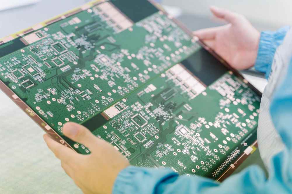
A PCB prototype service refers to the specialized manufacturing and assembly of small-batch printed circuit boards (PCBs) or printed circuit board assemblies (PCBAs) for testing and validation purposes. Unlike mass production, which focuses on scalability and cost-efficiency, prototyping prioritizes speed, flexibility, and accuracy—allowing engineers to verify design functionality, identify flaws, and make necessary adjustments before investing in large-scale production. The core purpose of prototyping is to de-risk your project: a high-quality prototype ensures that your design is manufacturable, performs as intended, and meets all technical requirements.
1.2 The Role of Prototyping in Reducing Risks & Accelerating Time-to-Market
Skipping or cutting corners on
PCB prototyping can lead to disastrous consequences. Imagine investing in mass production only to discover a critical design flaw that renders your product non-functional—this not only wastes time and money but also damages your brand reputation. Prototyping mitigates these risks by:
- Validating electrical performance (e.g., signal integrity, power distribution, impedance matching)
- Testing mechanical fit (e.g., compatibility with enclosures, component placement)
- Identifying manufacturability issues early (e.g., overly tight trace spacing, incompatible materials)
- Allowing for iterative improvements before full-scale production
By catching these issues in the prototyping phase, you can avoid costly retooling, reduce production delays, and bring your product to market faster than competitors who skip this vital step.
1.3 Common Challenges in PCB Prototyping
While prototyping offers immense value, it’s not without its challenges. Many engineers and product teams face common pain points such as:
- Design flaws that only surface during manufacturing (e.g., untested DFM compliance)
- Material mismatch (e.g., using standard FR4 for high-temperature applications)
- Delayed delivery due to inefficient service providers or poor communication
- Inconsistent quality that undermines testing validity
- Limited support for complex designs (e.g., multi-layer PCBs, HDI structures)
Understanding these challenges is the first step toward choosing a prototype service that can address them proactively.
1.4 What This Guide Will Cover
In this guide, we’ll dive deep into the key factors to evaluate when selecting a PCB prototype service, walk through the full manufacturing process from design submission to delivery, highlight common mistakes to avoid, and share insights on how to get the most out of your prototyping project. By the end, you’ll have the knowledge to partner with a service provider that delivers fast, high-quality prototypes—so you can move from concept to production with confidence.
二、Key Factors to Evaluate When Choosing a PCB Prototype Service
Not all PCB prototype services are created equal. To ensure your project’s success, you need to evaluate potential providers based on four critical pillars: technical capabilities, quality assurance, turnaround time, and service support.
2.1 Technical Capabilities
The technical expertise of your prototype service provider directly impacts the quality and functionality of your prototype. Key considerations include:
- Layer Count Support: Look for a provider that can handle your specific layer requirements, from single-layer PCBs for simple projects to 40-layer complex multi-layer PCBs for high-performance applications (e.g., aerospace, medical devices).
- Material Options: Ensure the provider offers a range of materials to match your project’s needs, including standard FR4, high Tg FR4 (for high-temperature environments), halogen-free FR4 (for environmental compliance), and high-frequency materials (e.g., Rogers) for RF/microwave applications.
- Precision & Tolerance: Ask about minimum trace width/spacing (e.g., 3mil/3mil) and hole size accuracy—critical for dense, high-precision designs. Tighter tolerances ensure that your prototype matches your design specifications and performs as expected.
- Special Process Support: If your project requires advanced processes (e.g., impedance control for signal integrity, blind/buried vias for space-saving, HDI for high-density designs), confirm that the provider has the equipment and expertise to deliver these capabilities.
2.2 Quality Assurance & Reliability
A prototype is only valuable if it’s reliable and consistent. Look for a service provider with a robust quality assurance (QA) system that includes:
- DFM Pre-Analysis: The best providers offer free Design for Manufacturability (DFM) analysis to identify potential issues before production starts—saving you time and avoiding costly reworks.
- Multi-Dimensional Testing: Quality prototypes require rigorous testing, including Automated Optical Inspection (AOI) for surface defects, X-Ray inspection for hidden issues (e.g., BGA solder joints), and continuity testing to ensure electrical connectivity.
- Compliance with International Standards: Ensure the provider adheres to industry standards such as IPC-A-610 (for PCB assembly) and ISO9001 (for quality management systems). Compliance guarantees that your prototype meets global quality benchmarks.
- Yield Rate & Defect Rate Guarantee: A reputable provider will stand behind their work with a clear yield rate guarantee (e.g., 99.8%+ for prototypes) and a low defect rate—giving you confidence in the reliability of your test results.
2.3 Turnaround Time & Flexibility
In the competitive electronics industry, speed matters. When evaluating prototype services, consider:
- Rapid Prototyping Options: Look for express service tiers (e.g., 24H, 48H, 72H turnaround) to meet tight deadlines. Fast prototyping allows you to iterate quickly and stay ahead of schedule.
- Small Batch Prototyping Support: Most prototyping projects require small quantities (1-100 units) for testing. Ensure the provider can handle small batches without sacrificing quality or charging exorbitant fees.
- Customization Flexibility: Your project may require custom specifications, such as unique board thickness (0.2mm-8.0mm), copper thickness (1oz-12oz), or solder mask color (green, black, red, etc.). A flexible provider will accommodate these requests to match your design needs.
2.4 Service & Support
Exceptional technical capabilities mean little without strong customer support. Look for a provider that offers:
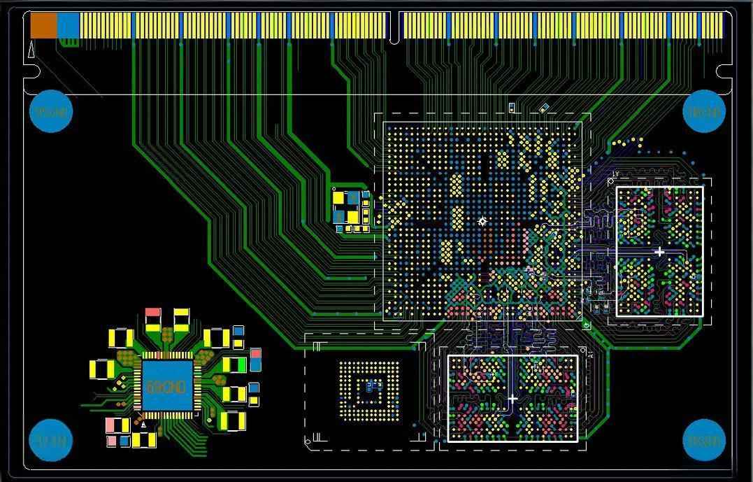
- File Review & Technical Consultation: The provider should review your design files (Gerber, BOM, assembly drawing) for compatibility and offer technical advice to optimize your design for manufacturing.
- Real-Time Order Tracking & Communication: Transparency is key—you should be able to track your order’s progress online and communicate with the team if issues arise.
- Post-Delivery Technical Support & Rework Assistance: If your prototype has issues or requires adjustments, the provider should offer prompt technical support and rework services to get your project back on track.
三、PCB Prototype Manufacturing Process: From Design to Delivery
Understanding the PCB prototype manufacturing process helps you set realistic expectations and collaborate more effectively with your service provider. Here’s a step-by-step breakdown:
3.1 Pre-Production Phase
The pre-production phase is critical for ensuring a smooth manufacturing process. Key steps include:
- Design File Submission & Verification: You’ll need to submit your design files in standard formats (e.g., Gerber RS-274X, BOM in Excel/CSV, assembly drawing in PDF). The provider will verify that the files are complete and compatible with their manufacturing equipment.
- DFM Analysis & Design Optimization Suggestions: The provider’s engineering team will conduct a DFM analysis to identify potential issues (e.g., insufficient trace spacing, incorrect pad sizes) and suggest optimizations to improve manufacturability.
- Material Selection & Confirmation: You’ll finalize material choices (e.g., FR4 high Tg, ENIG surface finish) based on your project’s requirements, and the provider will confirm availability and lead times.
3.2 Production Phase
Once pre-production is complete, the manufacturing process begins:
- PCB Fabrication Steps: The core fabrication process includes cutting the raw material (e.g., FR4 panel) to size, drilling holes (for vias and component leads), etching the copper layers to create traces, plating (to enhance conductivity), applying solder mask (to protect the board), and adding silkscreen (for component labeling).
- Assembly Process (for PCBA Prototypes): If you’re ordering a PCBA prototype, the provider will perform SMT (Surface Mount Technology) placement for small components (e.g., resistors, capacitors) and DIP (Dual In-Line Package) insertion for through-hole components. This is followed by soldering (wave soldering for DIP, reflow soldering for SMT) to secure components to the board.
- In-Process Quality Inspection: Quality checks are performed at key stages (e.g., after etching, after soldering) to ensure that each step meets specifications. This includes AOI inspection for surface defects and X-Ray inspection for BGA solder joints.
3.3 Post-Production Phase
The final phase focuses on testing, packaging, and delivery:
- Final Testing & Quality Validation: The completed prototype undergoes final testing, including continuity testing (to check for open/short circuits), functional testing (to verify performance), and visual inspection (to ensure compliance with IPC standards).
- Packaging & Shipping: Prototypes are packaged in anti-static bags to protect against electrostatic damage, then shipped via fast logistics (e.g., DHL, FedEx) to ensure timely delivery. Most providers offer tracking information so you can monitor your order’s journey.
四、Common Mistakes to Avoid in PCB Prototyping
Even with the best service provider, mistakes in the prototyping process can lead to delays and additional costs. Here are five common pitfalls to avoid:
4.1 Design-Related Mistakes
Many prototyping issues stem from design flaws that could have been avoided. Common design mistakes include:
- Insufficient trace spacing (leading to short circuits during manufacturing)
- Incorrect pad sizes (causing poor solder joints or component misalignment)
- Missing or incorrect reference designators (making assembly and testing difficult)
- Ignoring thermal management (leading to overheating in high-power applications)
To avoid these issues, always follow DFM guidelines and have your design reviewed by a technical expert before submission.
4.2 Material Selection Errors
Choosing the wrong material for your prototype can render your test results invalid. For example:
- Using standard FR4 (Tg 130°C) for high-temperature applications (e.g., automotive under-the-hood components) will lead to board warping or failure.
- Opting for a low-cost surface finish (e.g., HASL) for fine-pitch components may cause solder bridging or poor wetting.
Always match your material selection to your project’s operating environment, component type, and performance requirements.
4.3 Ignoring DFM Guidelines
Design for Manufacturability (DFM) is not just a buzzword—it’s a critical practice that ensures your design can be manufactured efficiently and accurately. Ignoring DFM guidelines (e.g., not leaving enough space for solder paste, designing non-standard hole sizes) can lead to unmanufacturable prototypes or costly reworks. Always work with a provider that offers DFM analysis and follow their recommendations.
4.4 Miscommunication with Prototyping Service Providers
Poor communication can lead to misunderstandings and prototype discrepancies. To avoid this:
- Clearly communicate your technical requirements (e.g., layer count, material, tolerance) upfront.
- Provide complete and accurate design files (double-check for missing layers or incorrect BOM entries).
- Ask questions if you’re unsure about any aspect of the process (e.g., lead times, testing methods).
A good service provider will proactively communicate with you, but it’s important to be clear about your expectations from the start.
4.5 How to Troubleshoot Common Prototype Defects
Even with careful planning, you may encounter defects in your prototype. Common issues include:
- Short circuits (often caused by insufficient trace spacing or solder bridging)
- Open circuits (resulting from poor soldering or broken traces)
- Poor solder joints (due to incorrect pad sizes or contaminated components)
- Board warping (from improper material selection or manufacturing processes)
If you encounter these issues, work with your service provider to troubleshoot: they can analyze the defect, identify the root cause (e.g., design flaw, manufacturing error), and suggest corrective actions (e.g., design revision, rework).
五、FAQs About PCB Prototype Service
To address common questions about PCB prototyping, we’ve compiled a list of frequently asked questions:
6.1 How Long Does PCB Prototyping Take?
Turnaround time depends on the provider, complexity of your design, and service tier. Most providers offer:
- Express service: 24H-72H for simple to moderately complex PCBs
- Standard service: 5-7 business days
- Complex designs (e.g., 20+ layers, HDI): 7-10 business days
Be sure to confirm lead times upfront, especially if you have tight deadlines.
6.2 What Files Do I Need to Provide for Prototyping?
For PCB prototyping, you’ll typically need to provide:
- Gerber files (RS-274X format) – the industry standard for PCB manufacturing
- Bill of Materials (BOM) – listing all components, part numbers, and quantities
- Assembly drawing (optional but recommended) – showing component placement and orientation
Some providers also accept CAD files (e.g., Altium, KiCad) for direct conversion to Gerber.
6.3 Can I Get a Custom Material for My PCB Prototype?
Yes, most reputable providers offer custom material options, including:
- High Tg FR4 (Tg 150°C-180°C) for high-temperature applications
- Halogen-free FR4 for environmental compliance (RoHS, REACH)
- High-frequency materials (e.g., Rogers, Taconic) for RF/microwave designs
- Flexible PCBs (FPC) for applications requiring bendability
Be sure to confirm material availability and lead times for custom requests.
6.4 How to Ensure the Prototype Matches My Design Requirements?
To ensure your prototype aligns with your design:
- Provide complete and accurate design files
- Work with a provider that offers DFM analysis and design verification
- Request a sample or test report (e.g., AOI results, continuity test) before full production
- Communicate any special requirements (e.g., tolerance, testing) upfront
A reliable provider will also offer a quality guarantee, so you can request rework if the prototype doesn’t meet your specifications.
6.5 What Is the Difference Between PCB Prototype and Mass Production?
PCB prototyping and mass production differ in several key ways:
- Quantity: Prototyping focuses on small batches (1-100 units), while mass production involves thousands or millions of units.
- Speed vs. Cost: Prototyping prioritizes speed and flexibility (higher per-unit cost), while mass production prioritizes scalability and cost-efficiency (lower per-unit cost).
- Process: Prototyping may use simplified processes (e.g., manual assembly for small batches), while mass production uses automated equipment for consistency.
- Purpose: Prototyping is for testing and validation, while mass production is for commercial distribution.
六、Choose FR4PCB.TECH for Your PCB Prototype Service: Fast, Reliable, and Expertly Crafted
When it comes to PCB prototyping, you need a partner that combines technical expertise, strict quality control, and responsive service—so you can focus on what you do best: innovating. At FR4PCB.TECH, we’ve built our reputation on delivering high-quality PCB and PCBA prototypes that meet the most demanding requirements of electronics engineers and product teams worldwide.
About FR4PCB.TECH
FR4PCB.TECH is a leading provider of one-stop
PCB manufacturing, prototyping, and assembly services. With years of experience in the electronics industry, we specialize in supporting projects from prototype to mass production, offering technical capabilities that include 2-98 layer PCB fabrication, high Tg/halogen-free/high-frequency material options, precision
SMT/DIP assembly, and advanced processes like impedance control and HDI. Our strict quality control system—including DFM pre-analysis, AOI/X-Ray/ICT testing, and compliance with IPC-A-610 and ISO9001 standards—ensures a stable product yield of 99.8%+, so you can trust that your prototype will perform as expected.
Our PCB Prototype Service Highlights
What sets us apart from other providers?
- 24H Express Prototyping: Get your simple to moderately complex PCB prototype in as little as 24 hours—perfect for tight deadlines.
- Free DFM Analysis: Our engineering team reviews your design files for free, identifying potential issues and offering optimization suggestions to improve manufacturability.
- One-Stop PCBA Prototyping: We handle everything from PCB fabrication to component sourcing, assembly, and testing—saving you time and eliminating the need to coordinate with multiple vendors.
- Fast Quotation: Receive a detailed quote within 2 hours of submitting your files, with transparent pricing and no hidden fees.
- 24/7 Technical Support: Our team of skilled engineers is available around the clock to answer your questions, troubleshoot issues, and provide guidance throughout the prototyping process.
Exclusive Offer for New Customers
To help you get started, we’re offering an exclusive discount for first-time customers: 10% off your first PCB or PCBA prototype order. Simply mention this offer when requesting a quote, and our team will apply the discount to your order.
Ready to turn your design concept into a high-quality prototype that accelerates your path to production? Partnering with FR4PCB.TECH means you’re not just getting a prototype—you’re getting a dedicated team of experts committed to your project’s success. Here’s how to get started in three simple steps:
- Upload Your Design Files: Visit our website at FR4PCB.TECH and navigate to the “PCB Prototype” section. Upload your Gerber files, BOM, and assembly drawing (if available) using our secure file submission portal. We accept all standard formats and provide instant file validation to ensure completeness.
- Receive Your Custom Quote: Our system will generate a detailed quote within 2 hours—no hidden fees, no surprises. You’ll see a breakdown of costs for fabrication, assembly (if needed), testing, and shipping, along with estimated delivery times based on your chosen service tier (24H express, standard, or complex design).
- Confirm & Launch Production: Once you approve the quote, our engineering team will immediately begin DFM analysis (free of charge) and prepare for production. You’ll receive real-time order tracking updates, so you always know where your prototype stands. We’ll also notify you once production is complete and your prototype is shipped via your preferred logistics partner (DHL, FedEx, or local courier).
Whether you’re working on a simple single-layer PCB or a complex 40-layer HDI prototype, FR4PCB.TECH has the technical capabilities, quality control, and speed to meet your needs. Our 24/7 technical support team is always available to answer questions, address concerns, or provide design guidance—so you can move forward with confidence.
Don’t let prototyping delays or quality issues hold back your project. Take advantage of our exclusive 10% discount for new customers and experience the FR4PCB.TECH difference today. Upload your files, get your quote, and let’s bring your innovation to life—one high-quality prototype at a time.
Visit FR4PCB.TECH now to start your prototype order, or contact our sales team at
info@fr4pcb.tech /
+86 18123677761 for personalized assistance. We can’t wait to be your trusted partner for PCB prototyping, manufacturing, and assembly—from concept to mass production.


