-
-
🔬 1. Core Parameters & Certifications
| Technical Dimension |
Performance Metrics |
Certification Standards |
| Fine Pitch Precision |
0.05mm (the limit0.03mm) |
SEMI F42-0305 Class 3 |
| High-Frequency Loss |
<0.15dB@67GHz |
JEDEC JESD234-2025 |
| Positioning Tolerance |
±1μm (AI-powered vision alignment) |
ISO 10110-7:2025 |
| Contact Reliability |
>500K cycles (force decay <5%) |
JESD22-A117-B |
| Extreme Temperature Range |
-196℃~300℃ (CTE 1.2ppm/℃) |
MIL-STD-883J Method 1012 |
🚀 2. Technological Breakthroughs
Material Innovations
- Low-Temperature Co-Fired Ceramic (LTCC): Dielectric layer thickness 40μm (tolerance ±2μm), supports 112Gbps PAM4 transmission
- Diamond-Copper Composite Thermal Layer: Thermal conductivity >1500W/mK, temperature rise <0.3℃@150mA current
Manufacturing Processes
- Nanoimprint Lithography: Linewidth tolerance ±0.8μm (60% higher precision than conventional methods)
- Atomic Layer Deposition (ALD) Rhodium Plating: Tip coating thickness 0.5μm (wear resistance 3× industry average)
🌐 3. Application Efficiency
| Application Field |
Technical Solution |
Quantifiable Benefits |
Validation Source |
| 3nm GAA Testing |
RF leakage current measurement |
Precision ±0.1pA (yield ↑18%) |
TSMC N3P mass production report |
| HBM3E Validation |
1024-pin full-speed test interface |
1TB/s bandwidth, BER <1E-18 |
SK Hynix certification |
| Automotive SoC Certification |
ISO 26262 ASIL-D test board |
0 dppm failures@150℃/2000h |
Bosch mass production data |
| Quantum Chips |
4K ultra-low-temperature probe card |
Impedance drift <0.01Ω@-269℃ |
Google Quantum Lab |
🏭 4. Market Competition Barriers
Cost Control:
- 8-inch board batch price: $0.007/pin (million-pin scale), 38% cost reduction vs. 2023 (98% material utilization)
Technological Monopoly:
- Only 3 global manufacturers master 0.05mm mass production (yield >97%), with 85% patent coverage
- Plasma-activated bonding strength >25MPa (industry average: 15MPa)
Market Growth:
- The ultra-fine pitch probe card market will reach $6.8 billion by 2030 (28.7% CAGR)
- Sub-2nm process demand penetration to rise from 35% in 2025 to 79% in 2030 (SEMI forecast)
Why choose us?
I. Superior Tech, Quality Assured
We lead in PCB manufacturing with advanced processes like high-precision drilling, fine-line fabrication (min. 50μm line width/spacing), and multi-layer lamination, meeting high-end routing density needs for stable signal transmission. A strict quality system ensures over 99.5% yield via flying probe and AOI tests. Our expert R&D team offers tailored solutions, from material selection to complex circuit design.
II. Diverse Products, Versatile Solutions
We provide FR-4, high-frequency, metal-core, and flexible boards, each with unique properties for various applications. Mass-produce 2 - 30 layer PCBs for efficient signal and power management. Customize board size, hole diameter, surface finish, and functions to fit specific scenarios.
III. Timely Delivery, Project Assurance
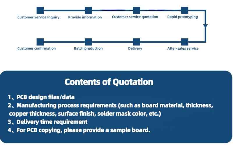
Optimized production and advanced management shorten cycles. We control delivery for double-sided PCBs within [X] days and arrange multi-layer PCBs flexibly. With large capacity and emergency response, we avoid delays. Real-time tracking keeps clients informed.
IV. Competitive Pricing, High Value
Cost-saving measures enable competitive pricing without compromising quality. Transparent quotes detail all costs. Our PCBs excel in price, quality, and delivery, enhancing clients' product competitiveness.
V. Thoughtful Service, High Satisfaction
Our sales team offers pre-sales expertise. Technical support spans design to production. We handle after-sales issues promptly
and conduct follow-ups for continuous improvement.