Pushing the Limits: Reliable Assembly of 01005 Components and 0.2mm Pitch BGAs
Introduction: The Irreversible Wave of Electronics Miniaturization
In today's rapidly evolving electronics industry, miniaturization has transcended mere trend status to become a survival imperative. Market research indicates global wearable device shipments surpassed 500 million units in 2023, with a compound annual growth rate exceeding 15%. The medical electronics sector shows even more aggressive demand for miniaturized devices, growing at approximately 20% annually. These figures reflect consumers' relentless pursuit of portability, comfort, and functional integration.
As smartphone thickness has been reduced to under 8mm, TWS earbuds have shrunk by nearly 40% compared to first-generation models, and implantable medical devices must deliver complex functionality within mere cubic millimeters, electronics miniaturization has entered uncharted territory. This trajectory directly drives components toward dimensional extremes: from early 1206 and 0805 packages, through mainstream 0402 and 0201 sizes, to today's cutting-edge 01005 components (0.4×0.2mm), with even 008004 packages (0.25×0.125mm) now in development. Simultaneously, high-performance chip packaging faces similar challenges, with BGA ball pitches shrinking from 1.0mm and 0.8mm to today's 0.4mm and 0.3mm, now reaching the bleeding edge of 0.2mm. While these technological leaps deliver enhanced performance, they simultaneously present unprecedented challenges for PCB assembly processes.
What are 01005 and 0.2mm-pitch BGA/QFP? What are the technical challenges?
The 01005-package component is one of the smallest passive components currently available on the market, with dimensions of just 0.4mm x 0.2mm. This means they are not only difficult to identify with the naked eye but also require extremely high precision during the placement process. Any slight deviation can lead to soldering issues, such as tombstoning or dry joints. For 0.2mm-pitch BGA/QFPs, the distance between adjacent solder balls is extremely small. This necessitates highly precise stencil aperture design and requires meticulous temperature control during the reflow soldering process to prevent problems like bridging or voids.
The Physical Limits of 01005/01015 Components
At just 0.4×0.2mm, 01005 components occupy merely 1/20th the volume of traditional 0402 parts, weighing less than 0.001 grams. These components confront multiple physical constraints: first, their dimensions approach the human eye's resolution limit (~0.1mm), making accurate positioning difficult for conventional vision systems; second, their dramatically increased surface-area-to-volume ratio intensifies electrostatic adhesion effects, causing components to be attracted to incorrect positions; third, during reflow soldering, unbalanced surface tension frequently triggers "tombstoning," where one end lifts off the pad.
Even more challenging are 01015 components (0.25×0.125mm), which push these difficulties to extremes. Their pad dimensions often fall below 75μm, imposing near-impossible demands on PCB design, stencil aperture precision, and component placement accuracy.
0.2mm Pitch BGA: The Dual Challenge of Precision and Reliability
0.2mm pitch BGAs represent the pinnacle of current packaging technology, with adjacent solder balls spaced merely three times the diameter of a human hair (~70μm). Within this microscopic landscape, conventional assembly processes face severe challenges:
- Stencil aperture precision: Requires ±5μm accuracy while maintaining appropriate area ratios (>0.66) to ensure proper solder paste release
- Ball coplanarity: BGA solder ball height variations must be controlled within 10μm to prevent partial solder joint failures
- Thermal management complexity: Dense solder joint distribution creates uneven thermal mass, dramatically increasing reflow profile optimization difficulty
- Inspection blind spots: Conventional AOI cannot inspect BGA underside joints, requiring X-ray or cross-section analysis that complicates quality control
How does FR4PCB.TECH overcome these high-precision assembly challenges?
To overcome these challenges, FR4PCB.TECH has implemented comprehensive technological innovations, establishing a high-reliability micro-assembly process platform:
1. Ultra-Precision Placement Systems
Next-generation high-accuracy pick-and-place machines equipped with 0.5μm resolution linear encoders and sub-pixel vision systems achieve ±10μm repeat placement accuracy under 6σ standards. For 01005 components, we've developed adaptive vacuum pressure pickup technology that monitors pickup force in real-time (0.1g precision) to prevent component damage or displacement during handling. Simultaneously, environmental control systems maintain workshop conditions at precisely 23±1°C and 45±5% RH, minimizing thermal expansion effects on placement accuracy.
2. Intelligent Solder Paste Printing Technology
Nanometer-grade laser-cut stencils (75μm thickness) with ±3μm aperture positioning accuracy feature trapezoidal sidewall designs to enhance solder paste release. Coupled with closed-loop controlled printers that monitor squeegee pressure (±0.5N accuracy) and separation speed (adjustable 0.1-5mm/s), we ensure solder paste volume consistency with CpK>1.67. Additionally, 3D solder paste inspection systems immediately verify volume, height, and offset after printing, creating real-time closed-loop quality control.
3. Optimized Nitrogen Reflow Soldering
Custom-developed nitrogen reflow ovens (oxygen content <50ppm) with 12 precisely controlled thermal zones maintain temperature uniformity within ±1°C. AI-driven profile optimization algorithms dynamically adjust heat distribution across regions with varying component density. For 0.2mm BGAs specifically, we employ a stepped ramp strategy: extending soak time between 150-180°C ensures proper flux activation, while precisely controlling time above liquidus (TAL) at 217°C+ to 45-60 seconds balances solder joint formation against thermal damage risks. Micro-zone thermocouple measurements verify BGA bottom temperature distribution, ensuring differentials remain under 3°C.
4. Comprehensive Quality Assurance System
We've established a four-tier inspection framework: 1) 3D SPI for solder paste quality verification; 2) high-resolution AOI (5μm pixel resolution) for component placement and preliminary solder joint assessment; 3) 3D X-ray (1μm resolution) for BGA void analysis and positional verification; 4) selective cross-sectioning for inaccessible areas. For 0.2mm BGAs, we've developed phase-contrast X-ray imaging technology that clearly distinguishes micro-bridging between adjacent solder balls, tripling detection capability compared to conventional methods.
Real-World Validation: In-Depth European Medical Client Case Study
A leading European cardiac monitoring device manufacturer planned to develop a next-generation implantable ECG monitor requiring 32-channel signal acquisition, wireless transmission, and six-month battery life within an 8×8×2mm package. The design incorporated 478 01005 components and two 136-ball 0.2mm pitch BGA processors, achieving component density of 185 units/cm²—far exceeding industry averages.
Challenges: The client required completion from prototype to FDA certification within 24 months, with first-run yield exceeding 95% to meet strict medical certification timelines. Additionally, ISO 13485 certification demands created exceptional traceability requirements.
Solutions:
- Implemented zoned thermal design with dedicated reflow profiles for BGA areas
- Developed custom fixtures to prevent flex PCB deformation during reflow
- Established board-level data tracking recording all process parameters and inspection results
- Implemented component moisture management following J-STD-033D standards for 01005 parts
Results: In the initial 500-unit production run, overall yield reached 98.7%, with BGA void rates controlled below 8% (significantly better than the 25% industry standard). This enabled the client to obtain FDA 510(k) certification 45 days ahead of schedule. Process capability analysis (Cp/Cpk>1.67) further validated production stability for subsequent volume manufacturing at 100,000 units monthly.
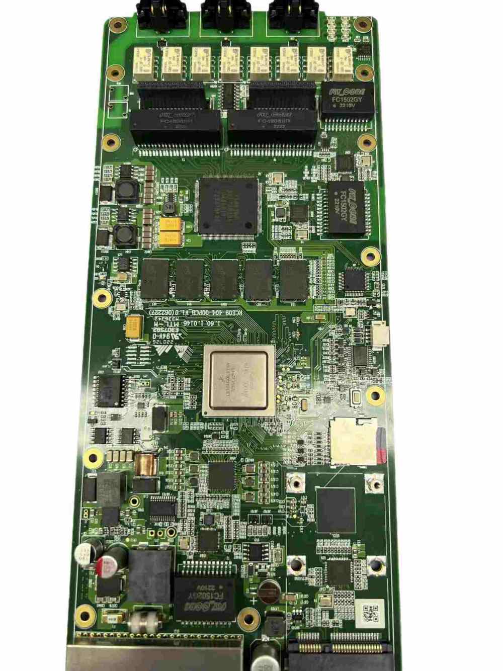
Future Outlook: Advancing Toward 008004 and 0.15mm BGA Era
Industry frontiers are already exploring 008004 components (0.25×0.125mm) and 0.15mm pitch BGAs. These technologies will demand placement accuracy entering the 5μm era, potentially requiring entirely new process paradigms such as wafer-level packaging (WLP) direct integration, microfluidic solder deposition, or selective laser soldering. Materials science breakthroughs will be equally critical—new solder alloys with low voiding characteristics and high reliability, plus advanced substrate materials with high-temperature resistance and low CTE will form essential foundations.
Conclusion: Exceeding Limits, Empowering Innovation
In electronics manufacturing, process capability often defines the boundaries of product innovation. When designers conceive miniaturized products, even the most brilliant concepts remain confined to paper without reliable manufacturing partners. FR4PCB.TECH is committed to becoming the solid backbone of electronics innovation—not only solving today's process challenges but also proactively developing next-generation manufacturing technologies. We believe that only by seamlessly connecting design creativity with manufacturing possibilities can we truly unlock electronics' innovative potential, transforming world-changing ideas from paper into reality.
Driven by the dual imperatives of miniaturization and performance enhancement, electronics manufacturing stands at a critical technological inflection point. Confronting extreme challenges like 01005 components and 0.2mm BGAs demands the integration of advanced equipment, materials science, process optimization, and quality control into systematic solutions. Only through such comprehensive approaches can we truly overcome miniaturization assembly barriers and pave the way for next-generation electronics. This represents not merely an evolution in manufacturing technology, but a crucial enabler for the entire electronics innovation ecosystem.
Why Choose FR4PCB.TECH?
✔ Deep expertise in FR4 materials = superior process stability
✔ MOQ of 1 piece; flexible volumes (1–5,000+)
✔ Transparent pricing, no hidden fees
✔ More than a manufacturer — your R&D ally
✔ Global free shipping for PCBA samples
— offering design review, supply chain optimization & tech insights
Core Technical Capabilities
✅ Advanced PCB Fabrication
-
Layers: 2–98 (specialized in 8–64)
-
Precision: 2mil/2mil, 0.1mm microvia
-
Processes: Blind/buried vias, thick copper (20oz), High-Tg/Rogers, ±3Ω impedance
✅ High-Precision PCBA Assembly
-
Smallest component: 01005, 0.2mm pitch BGA/QFP
-
Inspection: AOI + X-Ray + ICT + FCT
-
Compliance: IPC-A-610 Class 3, ESD-safe & dust-free environment
Who We Are?
-
12+ years specializing in complex PCB/PCBA prototyping & mass production
-
Served 1000+ global clients: defense, medical, automotive, industrial, R&D institutes
-
Core values: Technology-Driven · Full-Chain Collaboration · Rapid Response
FR4PCB.TECH – Your Trusted Partner for High-Difficulty PCB & PCBA Manufacturing and Turnkey Solutions
Accelerate Your Time-to-Market
📧 Email: info@fr4pcb.tech
🌐 Website: www.fr4pcb.tech
📍 Global Service · Made in China


